JFET
A JFET, or Junction Field-Effect Transistor, is a type of field-effect transistor. It is a voltage-controlled device that controls the current between two terminals by applying a voltage to a third terminal. JFETs are known for their high input impedance and are commonly used in applications requiring low noise and high-frequency performance.
Construction
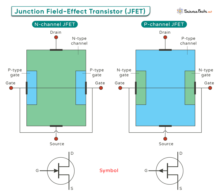
A JFET has three main terminals and a semiconductor channel, typically made from silicon or germanium. The three terminals are:
- Gate (G): It significantly controls the current flow through the JFET.
- Source (S): Carriers enter the channel through this region.
- Drain (D): Carriers leave the channel through this region.
The source and drain are located at the ends of the JFET and are connected by the channel. The gate is situated around or in the middle of the channel.
The schematics and symbols of the two types of JFET are shown in the diagram below.
How Does a JFET Work
A voltage is applied to the gate, which is reverse-biased relative to the source. It is known as the gate-source voltage.
This creates a depletion region within the channel that is void of charge carriers and non-conductive. The width of the depletion region increases with the magnitude of the reverse bias voltage.
In addition to the gate-source voltage, there is a drain-source voltage that creates an electric field, driving the current through the channel from the drain to the source.
As the gate-source voltage increases, the depletion region expands, narrowing the conductive channel. This narrowing restricts the flow of current from the drain to the source.
If the gate-source voltage is sufficiently high, the depletion regions from either side of the channel can meet. This phenomenon is known as “pinch-off”, and the channel severely restricts current flow. Beyond this point, the JFET enters saturation mode, where further increases in drain-source voltage do not significantly increase current flow.
Types
There are two main types of JFET: N-channel and P-channel.
1. N-Channel JFET
An N-Channel JFET has a channel composed of N-type semiconductor material, meaning that the majority charge carriers within the channel are electrons. N-channel JFETs typically exhibit higher electron mobility than P-channel JFETs, making them suitable for high-frequency applications.
2. P-Channel JFET
A P-Channel JFET features a channel made of P-type semiconductor material where the majority charge carriers are holes. While P-channel JFETs may not have the same electron mobility as N-channel devices, they are often used in low-power applications and can be advantageous in certain circuit configurations.
Therefore, due to its superior electron mobility, N-channel JFET is preferred for high-speed and high-frequency applications. P-channel JFET finds its niche in low-power circuits where hole conduction is beneficial.
I-V Characteristics
JFETs are important components in electronic circuits because of their unique current-voltage (I-V) characteristics.
Output or Drain Characteristics
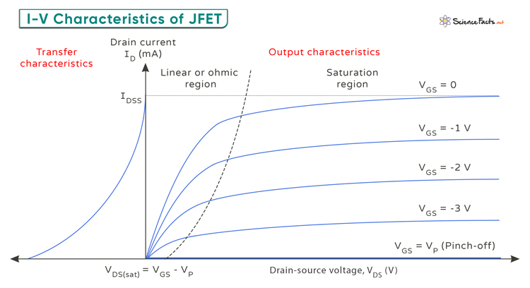
The output characteristics of a JFET show the relationship between the drain current (ID) and the drain-source voltage (VDS) while keeping the gate-source voltage (VGS) constant. These curves illustrate how ID changes with different VDS values, providing insights into the transistor’s behavior under various operating conditions.
Regions of Operation
The JFET exhibits varying characteristics at different stages of operation depending on the input voltages. Its characteristics in the different regions are described below.
1. Active or Saturation Region: The JFET operates as a constant-current source. Here, ID becomes relatively independent of VDS and is primarily controlled by the gate-source voltage VGS.
2. Ohmic Region: VDS is small, and ID increases linearly with VDS. The JFET behaves as a resistor whose value is controlled by VGS.
3. Cut-off or Pinch-off Region: VGS is sufficiently negative (for n-channel JFETs) or positive (for p-channel JFETs) to deplete the channel of carriers, effectively turning off the device. In this region, ID is minimal or zero, as the channel is fully pinched off.
Transfer Characteristics
The transfer characteristics describe the relationship between ID and VGS while keeping VDS constant. The transfer characteristics graph typically shows a curve that starts from ID at VGS = VP (pinch-off voltage). It rises as VGS becomes less negative (for n-channel) or less positive (for p-channel), demonstrating the inverse relationship between VGS and ID. As VGS approaches zero, ID reaches its maximum value, known as IDSS (drain current with gate shorted to source).
The graph below shows the I-V Characteristics of an N-channel JFET.
Applications
- Amplifiers: JFETs are commonly used as amplifiers in audio equipment, such as preamplifiers and signal amplifiers. Their high input impedance and low noise characteristics make them ideal for accurately amplifying weak signals.
- Switching Circuits: JFETs can be utilized as switches in electronic circuits where fast switching speeds are required. They can act as on-off switches by controlling the current flow through the device, making them essential components in digital logic circuits.
- Voltage Regulators: In voltage regulator circuits, JFETs help maintain a stable output voltage by adjusting the resistance based on the input voltage fluctuations. It ensures a consistent power supply, which is crucial for various electronic systems.
- Oscillators: JFETs are key in oscillator circuits that generate continuous waveforms at specific frequencies. These oscillators are vital components in communication systems, radars, and other electronic devices requiring precise frequency generation.
- Sensors: Due to their sensitivity to changes in electrical fields, JFETs are employed as sensors, such as pressure sensors, temperature sensors, and light sensors. They can convert physical quantities into electrical signals for monitoring and control purposes.
- Wireless Communications: JFETs excel at high-frequency operations due to their low capacitance values and minimal noise levels compared to other transistor types. It makes them suitable for radio frequency (RF) amplification in wireless communication systems.
-
References
Article was last reviewed on Friday, July 12, 2024

